JTAG (named after the Joint Test Action Group which codified it) is an industry standard for verifying designs and testing printed circuit boards after manufacture.
Processors often use JTAG to provide access to their debug/emulation functions and all FPGAs and CPLDs use JTAG to provide access to their programming functions.
JTAG implements standards for on-chip instrumentation in electronic design automation (EDA) as a complementary tool to digital simulation. It specifies the use of a dedicated debug port implementing a serial communications interface for low-overhead access without requiring direct external access to the system address and data buses.
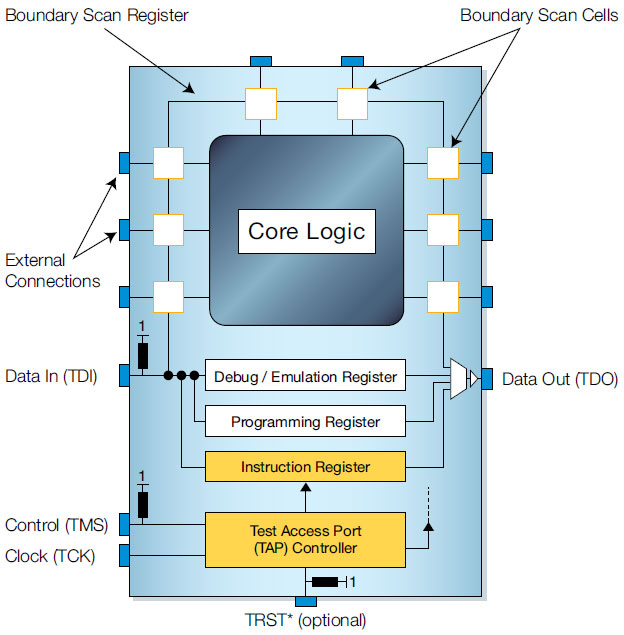
The interface connects to an on-chip test access port (TAP) that implements a stateful protocol to access a set of test registers that present chip logic levels and device capabilities of various parts.

Figure 1 – Schematic Diagram of a JTAG enabled device
The JTAG standards have been extended by many semiconductor chip manufacturers with specialized variants to provide vendor-specific features.
The debug and programming tools commonly associated with JTAG only make use of one aspect of the underlying technology – the four-wire JTAG communications protocol.
Description
- Debugs all ALTERA FPGA SOC microcontrollers with JTAG interface supported by Qartus II
- High speed USB 2.0 interface
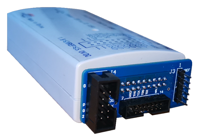
- Uses standard 2×10 PIN JTAG connector,can be extended to 14PIN,10PIN ,6PIN through adapter board.
- Working voltage range 1.8 – 5.0 V DC
- Dimensions 10.2×5.4 mm (2×1.6″) , Adapter plate (6pin, 2x7pin 2.54mm,15 cm (8″) 2×10 JTAG cable , 1×6 JTAG cable , 2×7 JTAG cable ribbon cable are included
