Codasip is proud to be a founding member of the RISC-V Foundation, joining industry leaders such as Google, Oracle, HP, AMD, Nvidia, and many others.
The power of RISC-V is that it defines an ISA that helps a healthy HW and SW ecosystems develop, allowing each vendor to deliver their own unique value. RISC-V ISA and related specifications are developed, ratified and maintained by RISC-V Foundation contributing members within the RISC-V Foundation Technical Committee. Operating details of the Technical Committee can be found in the RISC-V Foundation Tech Group. Work on the specification is performed on GitHub and the GitHub issue mechanism can be used to provide input into the specification.
1、Design Objective of the System
The main purpose of this system design is to complete FPGA learning, development and experiment with Intel Quartus.
The main device uses the Inte Cyclone10 10CL040YF484C8G and is currently the latest generation of FPGA devices from Intel. The major learning and development projects can be completed as follows:
- Basic FPGA design training
- Construction and training of the SOPC (NiosII) system
- IC design and verification, the system provides hardware design, simulation and verification of RISC-V CPU
- Development and application based on RISC-V
- The system is specifically optimized for hardware design for RISC-V system applications
RISC-V Board ( ARTIX 100T, XC7A100T ) – FII-PRX100 – Xilinx Risc-V FPGA Board ( riscv SOPC AI Xilinx artix-7 )
Xilinx and Altera Risc-V FPGA Board
2、System Resource
- Extended memory: Two Super Sram (IS61WV51216, 512K x 32bit) are connected in parallel to form a 32-bit data interface, and the maximum access space is up to 2M bytes.
- Serial flash: Spi interface serial flash (16M bytes)
- Serial EEPROM
- Gigabit Ethernet: 100/1000 Mbps
- USB to serial interface: USB-UART bridge
3、Human-computer Interaction Interface
- 8 DIP switches
- 8 push buttons, definition of 7 push buttons: MENU, UP, RETUN, LEFT, OK, RIGHT, DOWN, 1 for reset: RESET
- 8 LEDs
- 6 7-segment LED display
- I2C bus interface
- UART external interface
- Two JTAG programming interfaces: One is for downloading the FPGA debug interface, and the other is the JTAG debug interface for RISC-V CPU
- Built-in RISC-V CPU software debugger, no external RISC-V JTAG emulator required
- 4 12-pin GPIO connectors, in line with PMOD interface standards
Codasip’s RISC-V-based processors (Bk) make use of the rich ecosystem of software and hardware enabled by the extensible, RISC-V Instruction-Set Architecture (ISA) Standard, while retaining the incredible flexibility of all Codasip-made cores.
All Codasip Bk cores are fully customizable to the needs of your design. Changes can be made by Codasip as part of the standard deliverable, or by your own developers using our unique IP Generation Toolkit (Codasip Studio).
Need a single-cycle MAC, specialized crypto functions, or support for non-standard data types? No problem. Better yet, thanks to the extensible nature of the RISC-V ISA, all tailored cores remain RISC-V compliant, allowing you to use the growing SW Ecosystem.
4、Software Development System
- Quartus 18.0 and later version for FPGA development, Nios-II SOPC
- Freedom Studio-Win_x86_64 software development for RISC-V CPU
5、Supporting Resources
RISC-V JTAG Debugger Intel Altera JTAG Download Debugger FII-PRA040 User Experimental Manual FII-PRA040 Hardware Reference Guide
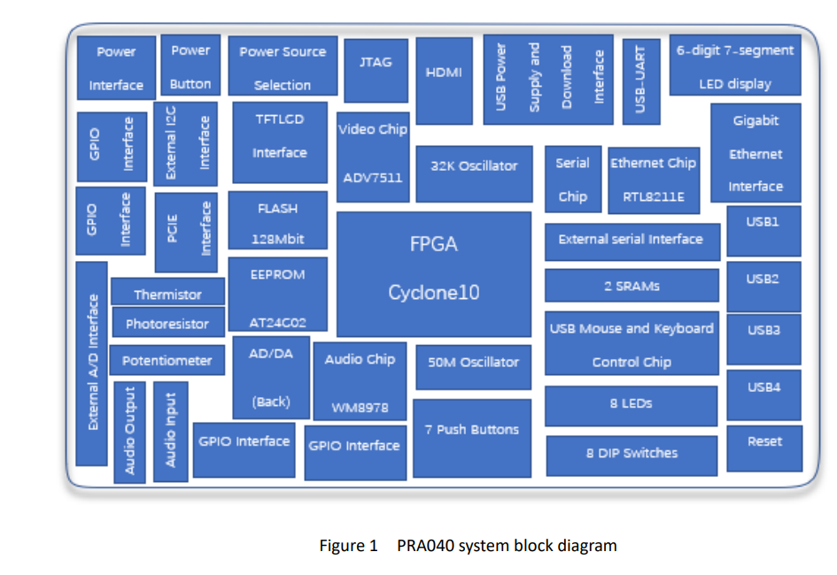
6、Physical Picture
Unlike other academic designs which are optimized only for simplicity of exposition, the designers state that the RISC-V instruction set is for practical computers. It is said to have features to increase computer speed, yet reduce cost and power use.
These include a load–store architecture, bit patterns to simplify the multiplexers in a CPU, simplified standards-based floating-point, a design that is architecturally neutral, and placing most-significant bits at a fixed location to speed sign extension. Sign extension is said to often be on the critical timing path.
The instruction set is designed for a wide range of uses. It is variable-width and extensible so that more encoding bits can always be added.
It supports three word-widths, 32, 64, and 128 bits, and a variety of subsets. The definitions of each subset vary slightly for the three word-widths. The subsets support small embedded systems, personal computers, supercomputers with vector processors, and warehouse-scale rack-mounted parallel computers.
The instruction set space for the 128-bit stretched version of the ISA was reserved because 60 years of industry experience has shown that the most unrecoverable error in instruction set design is a lack of memory address space. As of 2016, the 128-bit ISA remains undefined intentionally, because there is yet so little practical experience with such large memory systems. There are proposals to implement variable-width instructions up to 864-bits.
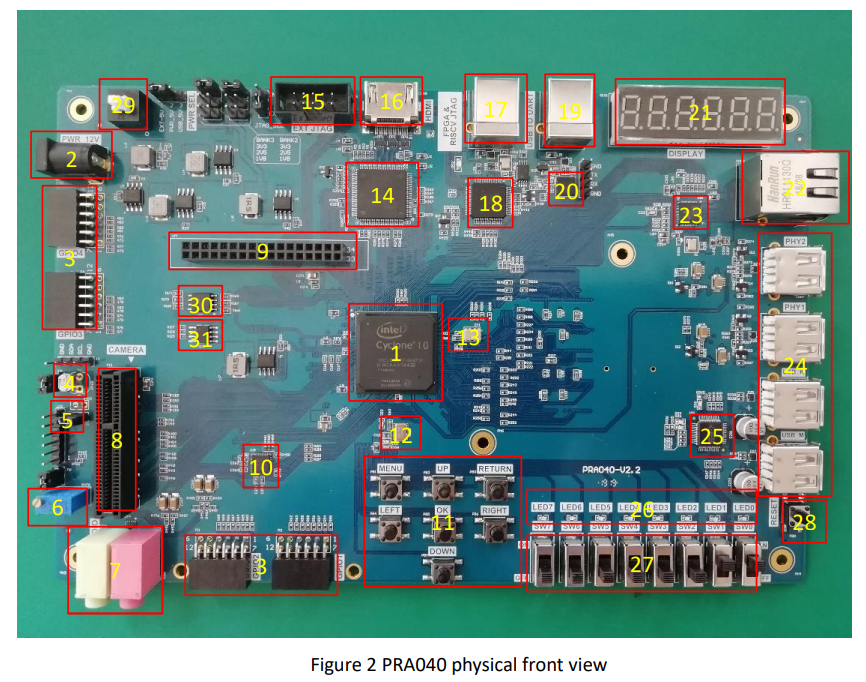
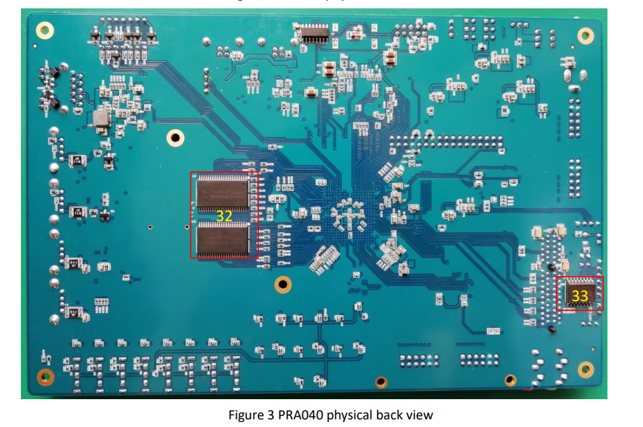
Corresponding to the physical picture, the main devices on board are as follows:
1、10CL040YE484C8G chip
2、External 12V power interface
3、GPIO interface
4、Thermistor (NTC-MF52)
5、Photoresistor
6、Potentiometer
7、Audio output (green), audio input (red)
8、PCIE interface
9、TFTCLD interface
10、Audio chip (WM8978)
11、7 push buttons
12、50M system clock
14、Video chip(ADV7511)
15、External JTAG download interface
16、HDMI interface
17、USB power supply and download interface
18、FPGA and RISC_V JTAG download chips (FT2232)
19、USB_UART interface
20、Serial chip (CP2102)
21、6 7-segment LED display
22、Ethernet interface
23、Ethernet PHY chip (RTL8211E-VB)
24、4 USB interfaces
25、USB mouse and keyboard control chip
26、8 LEDs
27、8-bit DIP switch
28、Reset button
29、Power button
30、Flash (N25Q128A,128M bit/16M bytes)
31、EEPROM (AT24C02N)
32、Two SRAMs
33、AD/DA conversion chip (PCF8591)
PRA040 Altera Risc-V FPGA Board Here
[display-posts posts_per_page=”20″]